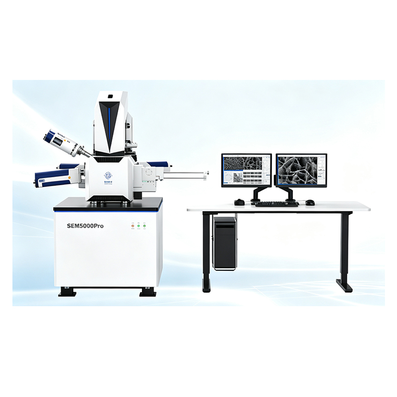
Adopting High‑Pressure Tunnel technology (Super‑Tunnel), crossover‑free electron optical path and electrostatic‑electromagnetic hybrid objective lens design, the instrument reduces space‑charge effect and system aberration, and achieves a resolution of 1.1 nm @ 1 kV.
With improved imaging resolution under low‑voltage conditions, it enables direct observation of non‑conductive or semiconductor samples and effectively reduces irradiation damage to specimens.